NAND gate
This article relies largely or entirely on a single source. (July 2023) |
| NAND gate truth table | ||
|---|---|---|
| Input | Output | |
| A | B | A NAND B |
| 0 | 0 | 1 |
| 0 | 1 | 1 |
| 1 | 0 | 1 |
| 1 | 1 | 0 |
In digital electronics, a NAND gate (NOT-AND) is a logic gate which produces an output which is false only if all its inputs are true; thus its output is complement to that of an AND gate. A LOW (0) output results only if all the inputs to the gate are HIGH (1); if any input is LOW (0), a HIGH (1) output results. A NAND gate is made using transistors and junction diodes. By De Morgan's laws, a two-input NAND gate's logic may be expressed as , making a NAND gate equivalent to inverters followed by an OR gate.
The NAND gate is significant because any Boolean function can be implemented by using a combination of NAND gates. This property is called "functional completeness". It shares this property with the NOR gate. Digital systems employing certain logic circuits take advantage of NAND's functional completeness.
NAND gates with two or more inputs are available as integrated circuits in transistor–transistor logic, CMOS, and other logic families.
Symbols
[edit]There are three symbols for NAND gates: the MIL/ANSI symbol, the IEC symbol and the deprecated DIN symbol sometimes found on old schematics. The ANSI symbol for the NAND gate is a standard AND gate with an inversion bubble connected.

|

|

|
| MIL/ANSI Symbol | IEC Symbol | DIN Symbol |
Logic
[edit]The function NAND(a1, a2, ..., an) is logically equivalent to NOT(a1 AND a2 AND ... AND an).
One way of expressing A NAND B is , where the symbol signifies AND and the bar signifies the negation of the expression under it: in essence, simply .
Implementations
[edit]The basic implementations can be understood from the image on the left below: If either of the switches S1 or S2 is open, the pull-up resistor R will set the output signal Q to 1 (high). If S1 and S2 are both closed, the pull-up resistor will be overridden by the switches, and the output will be 0 (low).
In the depletion-load NMOS logic realization in the middle below, the switches are the transistors T2 and T3, and the transistor T1 fulfills the function of the pull-up resistor.
In the CMOS realization on the right below, the switches are the n-type transistors T3 and T4, and the pull-up resistor is made up of the p-type transistors T1 and T2, which form the complement of transistors T3 and T4.
- Realization of NAND gates in different logic families
-
Implementation using switches and a pull-up resistor
In CMOS, NAND gates are more efficient than NOR gates. This is due to the faster charge mobility in n-MOSFETs compared to p-MOSFETs, so that the parallel connection of two p-MOSFETs (T1 and T2) realised in the NAND gate is more favourable than their series connection in the NOR gate. For this reason, NAND gates are generally preferred over NOR gates in CMOS circuits. [1]
Hardware design and pinout
[edit]
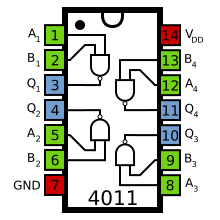
NAND gates are basic logic gates, and as such they are recognised in TTL and CMOS ICs.
The standard, 4000 series, CMOS IC is the 4011, which includes four independent, two-input, NAND gates. These devices are available from many semiconductor manufacturers. These are usually available in both through-hole DIL and SOIC formats. Datasheets are readily available in most datasheet databases.
The standard two-, three-, four- and eight-input NAND gates are available:
- CMOS
- 4011: Quad two-input NAND gate
- 4023: Triple three-input NAND gate
- 4012: Dual four-input NAND gate
- 4068: Mono eight-input NAND gate
- TTL
- 7400: Quad two-input NAND gate
- 7410: Triple three-input NAND gate
- 7420: Dual four-input NAND gate
- 7430: Mono eight-input NAND gate
Functional completeness
[edit]
The NAND gate has the property of functional completeness, which it shares with the NOR gate. That is, any other logic function (AND, OR, etc.) can be implemented using only NAND gates.[2] An entire processor can be created using NAND gates alone. In TTL ICs using multiple-emitter transistors, it also requires fewer transistors than a NOR gate.
As NOR gates are also functionally complete, if no specific NAND gates are available, one can be made from NOR gates using NOR logic.[2]
See also
[edit]References
[edit]- ^ Smith, J.S. "Digital circuits, sizing, output impedance, rise and fall time" (PDF). Archived from the original (PDF) on 2007-07-06.
- ^ a b Mano, M. Morris and Charles R. Kime. Logic and Computer Design Fundamentals, Third Edition. Prentice Hall, 2004. p. 73.
External links
[edit]- TTL NAND and AND gates at All About Circuits


