Lift-off (microtechnology)
This article needs additional citations for verification. (June 2011) |
The lift-off process in microstructuring technology is a method of creating structures (patterning) of a target material on the surface of a substrate (e.g. wafer) using a sacrificial material (e.g. photoresist). It is an additive technique as opposed to more traditional subtracting technique like etching. The scale of the structures can vary from the nanoscale up to the centimeter scale or further, but are typically of micrometric dimensions.
Process
[edit]
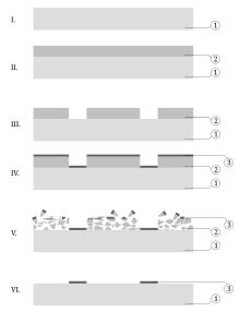
II. Deposition of the sacrificial stencil layer
III. Patterning the sacrificial layer (ex. etching), creating an inverse pattern
IV. Deposition of the target material
V. Washing out the sacrificial layer together with the target material on its surface
VI. Final pattern Layers:
1) Substrate
2) Sacrificial material
3) Target material
An inverse pattern is first created in the sacrificial stencil layer (ex. photoresist), deposited on the surface of the substrate. This is done by etching openings through the layer so that the target material can reach the surface of the substrate in those regions, where the final pattern is to be created. The target material is deposited over the whole area of the wafer, reaching the surface of the substrate in the etched regions and staying on the top of the sacrificial layer in the regions, where it was not previously etched. When the sacrificial layer is washed away (photoresist in a solvent), the material on the top is lifted-off and washed together with the sacrificial layer below. After the lift-off, the target material remains only in the regions where it had a direct contact with the substrate.
- Substrate is prepared
- Sacrificial layer is deposited and an inverse pattern is created (ex. photoresist is exposed and developed. Depending on the resist various methods can be used, such as Extreme ultraviolet lithography - EUVL or Electron beam lithography - EBL. The photoresist is removed in the areas, where the target material is to be located, creating an inverse pattern.)
- Target material (usually a thin metal layer) is deposited (on the whole surface of the wafer). This layer covers the remaining resist as well as parts of the wafer that were cleaned of the resist in the previous developing step.
- The rest of the sacrificial material (ex. photoresist) is washed out together with parts of the target material covering it, only the material that was in the "holes" having direct contact with the underlying layer (substrate/wafer) stays
Advantages
[edit]Lift-off is applied in cases where a direct etching of structural material would have undesirable effects on the layer below. Lift-off is a cheap alternative to etching in a research context, which permits a slower turn-around time. Finally, lifting off a material is an option if there is no access to an etching tool with the appropriate gases.
Disadvantages
[edit]There are 3 major problems with lift-off:
- Retention
- This is the worst problem for liftoff processes. If this problem occurs, unwanted parts of the metal layer will remain on the wafer. This can be caused by different situations. The resist below the parts that should have been lifted off could not have dissolved properly. Also, it is possible that the metal has adhered so well to the parts that should remain that it prevents lift-off.
- Ears
- When the metal is deposited, and it covers the sidewalls of the resist, "ears" can be formed. These are made of the metal along the sidewall which will be standing upwards from the surface. Also, it is possible that these ears will fall over on the surface, causing an unwanted shape on the substrate.
If the ears remain on the surface, the risk remains that these ears will go through different layers put on top of the wafer and they might cause unwanted connections.
- Redeposition
- During the liftoff process it is possible that particles of metal will become reattached to the surface, at a random location. It is very difficult to remove these particles after the wafer has dried.
Use
[edit]Lift-off process is used mostly to create metallic interconnections.
There are several types of lift-off processes, and what can be achieved depends highly on the actual process being used. Very fine structures have been used using EBL, for instance. The lift-off process can also involve multiple layers of different types of resist. This can for instance be used to create shapes that will prevent side walls of the resist being covered in the metal deposition stage.
