Draft:Direct Atomic Layer Processing
 | Draft article not currently submitted for review.
This is a draft Articles for creation (AfC) submission. It is not currently pending review. While there are no deadlines, abandoned drafts may be deleted after six months. To edit the draft click on the "Edit" tab at the top of the window. To be accepted, a draft should:
It is strongly discouraged to write about yourself, your business or employer. If you do so, you must declare it. Where to get help
How to improve a draft
You can also browse Wikipedia:Featured articles and Wikipedia:Good articles to find examples of Wikipedia's best writing on topics similar to your proposed article. Improving your odds of a speedy review To improve your odds of a faster review, tag your draft with relevant WikiProject tags using the button below. This will let reviewers know a new draft has been submitted in their area of interest. For instance, if you wrote about a female astronomer, you would want to add the Biography, Astronomy, and Women scientists tags. Editor resources
Last edited by Ivan.kundrata (talk | contribs) 3 seconds ago. (Update) |
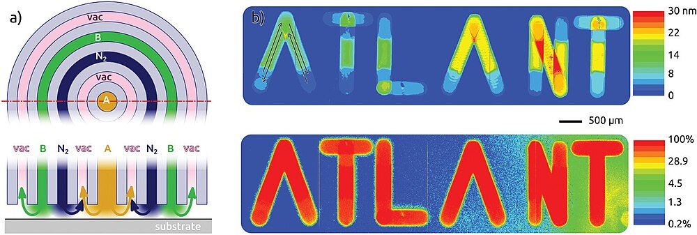
Direct Atomic layer processing(DALP), is a subset technique of Atomic Layer Deposition and Atomic Layer Etching, using exactly the same chemical processes. More specifically it is a subset of Spatial Atomic Layer deposition, where DALP is using micro-nozzles to have a fully constrained system in XYZ, essentially allowing for deposition with a micro-spot as seen on figure 1.

Introduction
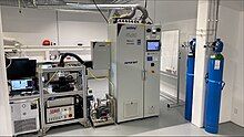
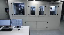
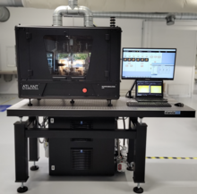
[edit]DALP has via the development of micro-nozzles and appropriate driving gas systems achieved direct processing, essentially allowing ALD and ALE to be used in an additive manufacturing mode. This work via the spatial ALD route, where the precursor and reactant combination of ALD/ALE is separated in space via gas dynamics as seen on figure 1. Currently DALP is being developed by the company ATLANT 3D Nanosystems and an FAU university group Chemistry of Thin Film Materials. See examples of micronozzles and machines to drive them on figures 2 to X.


History
[edit]1960s
[edit]2000s
[edit]Surface reaction mechanisms
[edit]Thermal ALD
[edit]Plasma ALD
[edit]Spatial ALD
[edit]Photo-assisted ALD
[edit]Metal ALD
[edit]Catalytic SiO2 ALD
[edit]Applications
[edit]Microelectronics applications
[edit]Gate oxides
[edit]Transition-metal nitrides
[edit]Metal films
[edit]Magnetic recording heads
[edit]DRAM capacitors
[edit]Photovoltaic Applications
[edit]Electrooptic Applications
[edit]Thin Film Couplers
[edit]Biomedical applications
[edit]As a permeation barrier for plastics
[edit]Quality and its control
[edit]Advantages and limitations
[edit]Advantages
[edit]Disadvantages
[edit]Economic viability
[edit]Reaction time
[edit]Chemical limitations
[edit]
