Waveguide (optics)
An optical waveguide is a physical structure that guides electromagnetic waves in the optical spectrum. Common types of optical waveguides include optical fiber waveguides, transparent dielectric waveguides made of plastic and glass, liquid light guides, and liquid waveguides.
Optical waveguides are used as components in integrated optical circuits or as the transmission medium in local and long-haul optical communication systems. They can also be used in optical head-mounted displays in augmented reality.[1]
Optical waveguides can be classified according to their geometry (planar, strip, or fiber waveguides), mode structure (single-mode, multi-mode), refractive index distribution (step or gradient index), and material (glass, polymer, semiconductor).
Total internal reflection
[edit]
The basic principles behind optical waveguides can be described using the concepts of geometrical or ray optics, as illustrated in the diagram.
Light passing into a medium with higher refractive index bends toward the normal by the process of refraction (Figure a.). Take, for example, light passing from air into glass. Similarly, light traveling in the opposite direction (from glass into air) takes the same path, bending away from the normal. This is a consequence of time-reversal symmetry. Each ray in air (black) can be mapped to a ray in the glass (blue), as shown in Figure b. There's a one-to-one correspondence. But because of refraction, some of the rays in the glass are left out (red). The remaining rays are trapped in the glass by a process called total internal reflection. They are incident on the glass-air interface at an angle above the critical angle. These extra rays correspond to a higher density of states in more-advanced formulations based on the Green's function.
Using total internal reflection, we can trap and guide the light in a dielectric waveguide (Figure c). The red rays bounce off both the top and bottom surface of the high index medium. They're guided even if the slab curves or bends, so long as it bends slowly. This is the basic principle behind fiber optics in which light is guided along a high index glass core in a lower index glass cladding (Figure d).
Ray optics only gives a rough picture of how waveguides work. Maxwell's equations can be solved by analytical or numerical methods for a full-field description of a dielectric waveguide.
Dielectric slab waveguide
[edit]This section needs additional citations for verification. (February 2021) |

Perhaps the simplest optical waveguide is the dielectric slab waveguide,[2] also called a planar waveguide.[3] Owing to their simplicity, slab waveguides are often used as toy models but also find application in on-chip devices like arrayed waveguide gratings and acousto-optic filters and modulators.
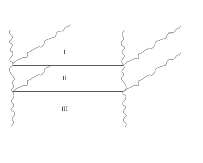
The slab waveguide consists of three layers of materials with different dielectric constants, extending infinitely in the directions parallel to their interfaces. Light is confined in the middle layer by total internal reflection if the refractive index of the middle layer is larger than that of the surrounding layers.
The slab waveguide is essentially a one-dimensional waveguide. It traps light only normal to the dielectric interfaces. For guided modes, the field in domain II in the diagram is propagating and can be treated as a plane wave. The field in domains I and III evanescently decay away from the slab. The plane wave in domain II bounces between the top and bottom interfaces at some angle typically specified by the , the wave vector in the plane of the slab. Guided modes constructively interfere on one complete roundtrip in the slab. At each frequency, one or more modes can be found giving a set of eigenvalues which can be used to construct a band diagram or dispersion relation.
Because guided modes are trapped in the slab, they cannot be excited by light incident on the top or bottom interfaces. Light can be end-fire or butte coupled by injecting it with a lens in the plane of the slab. Alternatively a coupling element may be used to couple light into the waveguide, such as a grating coupler or prism coupler.
There are 2 technologies: diffractive waveguides and reflective waveguides.
Two-dimensional waveguide
[edit]Strip waveguide
[edit]A strip waveguide is basically a strip of the layer confined between cladding layers. The simplest case is a rectangular waveguide, which is formed when the guiding layer of the slab waveguide is restricted in both transverse directions rather than just one. Rectangular waveguides are used in integrated optical circuits and in laser diodes. They are commonly used as the basis of such optical components as Mach–Zehnder interferometers and wavelength division multiplexers. The cavities of laser diodes are frequently constructed as rectangular optical waveguides. Optical waveguides with rectangular geometry are produced by a variety of means, usually by a planar process.[citation needed]
The field distribution in a rectangular waveguide cannot be solved analytically, however approximate solution methods, such as Marcatili's method,[4] Extended Marcatili's method[5] and Kumar's method,[6] are known.
Rib waveguide
[edit]A rib waveguide is a waveguide in which the guiding layer basically consists of the slab with a strip (or several strips) superimposed onto it. Rib waveguides also provide confinement of the wave in two dimensions and near-unity confinement is possible in multi-layer rib structures.[7]
Segmented waveguide and photonic crystal waveguide
[edit]Optical waveguides typically maintain a constant cross-section along their direction of propagation. This is for example the case for strip and of rib waveguides. However, waveguides can also have periodic changes in their cross-section while still allowing lossless transmission of light via so-called Bloch modes. Such waveguides are referred to as segmented waveguides (with a 1D patterning along the direction of propagation[8]) or as photonic crystal waveguides (with a 2D or 3D patterning[9]).
Laser-inscribed waveguide
[edit]Optical waveguides find their most important application in photonics. Configuring the waveguides in 3D space provides integration between electronic components on a chip and optical fibers. Such waveguides may be designed for a single mode propagation of infrared light at telecommunication wavelengths, and configured to deliver optical signal between input and output locations with very low loss.

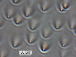
One of the methods for constructing such waveguides utilizes photorefractive effect in transparent materials. An increase in the refractive index of a material may be induced by nonlinear absorption of pulsed laser light. In order to maximize the increase of the refractive index, a very short (typically femtosecond) laser pulses are used, and focused with a high NA microscope objective. By translating the focal spot through a bulk transparent material the waveguides can be directly written.[10] A variation of this method uses a low NA microscope objective and translates the focal spot along the beam axis. This improves the overlap between the focused laser beam and the photorefractive material, thus reducing power needed from the laser.[11] When transparent material is exposed to an unfocused laser beam of sufficient brightness to initiate photorefractive effect, the waveguides may start forming on their own as a result of an accumulated self-focusing.[12] The formation of such waveguides leads to a breakup of the laser beam. Continued exposure results in a buildup of the refractive index towards the centerline of each waveguide, and collapse of the mode field diameter of the propagating light. Such waveguides remain permanently in the glass and can be photographed off-line (see the picture on the right).
Light pipe
[edit]Light pipes are tubes or cylinders of solid material used to guide light a short distance. In electronics, plastic light pipes are used to guide light from LEDs on a circuit board to the user interface surface. In buildings, light pipes are used to transfer illumination from outside the building to where it is needed inside.[citation needed]
Optical fiber waveguide
[edit]
Optical fiber is typically a circular cross-section dielectric waveguide consisting of a dielectric material surrounded by another dielectric material with a lower refractive index. Optical fibers are most commonly made from silica glass, however other glass materials are used for certain applications and plastic optical fiber can be used for short-distance applications.[citation needed]
See also
[edit]- ARROW waveguide
- Cutoff wavelength
- Dielectric constant
- Digital planar holography
- Electromagnetic radiation
- Equilibrium mode distribution
- Erbium-doped waveguide amplifier
- Leaky mode[13]
- Lightguide display
- Photonic crystal
- Photonic-crystal fiber
- Prism coupler
- Transmission medium
- Waveguide (radio frequency)
- Waveguide
- Zero-mode waveguide
References
[edit]- ^ Xiong, Jianghao; Hsiang, En-Lin; He, Ziqian; Zhan, Tao; Wu, Shin-Tson (2021-10-25). "Augmented reality and virtual reality displays: emerging technologies and future perspectives". Light: Science & Applications. 10 (1): 216. Bibcode:2021LSA....10..216X. doi:10.1038/s41377-021-00658-8. ISSN 2047-7538. PMC 8546092. PMID 34697292.
- ^ Ramo, Simon, John R. Whinnery, and Theodore van Duzer, Fields and Waves in Communications Electronics, 2 ed., John Wiley and Sons, New York, 1984.
- ^ "Silicon Photonics", by Graham T. Reed, Andrew P. Knights
- ^ Marcatili, E. A. J. (1969). "Dielectric rectangular waveguide and directional coupler for integrated optics". Bell Syst. Tech. J. 48 (7): 2071–2102. doi:10.1002/j.1538-7305.1969.tb01166.x.
- ^ Westerveld, W. J., Leinders, S. M., van Dongen, K. W. A., Urbach, H. P. and Yousefi, M (2012). "Extension of Marcatili's Analytical Approach for Rectangular Silicon Optical Waveguides". Journal of Lightwave Technology. 30 (14): 2388–2401. arXiv:1504.02963. Bibcode:2012JLwT...30.2388W. doi:10.1109/JLT.2012.2199464. S2CID 23182579.
{{cite journal}}: CS1 maint: multiple names: authors list (link) - ^ Kumar, A., K. Thyagarajan and A. K. Ghatak. (1983). "Analysis of rectangular-core dielectric waveguides—An accurate perturbation approach". Opt. Lett. 8 (1): 63–65. Bibcode:1983OptL....8...63K. doi:10.1364/ol.8.000063. PMID 19714136.
{{cite journal}}: CS1 maint: multiple names: authors list (link) - ^ Talukdar, Tahmid H.; Allen, Gabriel D.; Kravchenko, Ivan; Ryckman, Judson D. (2019-08-05). "Single-mode porous silicon waveguide interferometers with unity confinement factors for ultra-sensitive surface adlayer sensing". Optics Express. 27 (16): 22485–22498. Bibcode:2019OExpr..2722485T. doi:10.1364/OE.27.022485. ISSN 1094-4087. OSTI 1546510. PMID 31510540.
- ^ M. Hochberg; T. Baehr-Jones; C. Walker; J. Witzens; C. Gunn; A. Scherer (2005). "Segmented Waveguides in Thin Silicon-on-Insulator" (PDF). Journal of the Optical Society of America B. 22 (7): 1493–1497. Bibcode:2005JOSAB..22.1493H. doi:10.1364/JOSAB.22.001493.
- ^ S. Y. Lin; E. Chow; S. G. Johnson; J. D. Joannopoulos (2000). "Demonstration of highly efficient waveguiding in a photonic crystal slab at the 1.5-μm wavelength". Optics Letters. 25 (17): 1297–1299. Bibcode:2000OptL...25.1297L. doi:10.1364/ol.25.001297. OSTI 754329. PMID 18066198.
- ^ Meany, Thomas (2014). "Optical Manufacturing: Femtosecond-laser direct-written waveguides produce quantum circuits in glass". Laser Focus World. 50 (7).
- ^ Streltsov, AM; Borrelli, NF (1 January 2001). "Fabrication and analysis of a directional coupler written in glass by nanojoule femtosecond laser pulses". Optics Letters. 26 (1): 42–3. Bibcode:2001OptL...26...42S. doi:10.1364/OL.26.000042. PMID 18033501.
- ^ Khrapko, Rostislav; Lai, Changyi; Casey, Julie; Wood, William A.; Borrelli, Nicholas F. (15 December 2014). "Accumulated self-focusing of ultraviolet light in silica glass". Applied Physics Letters. 105 (24): 244110. Bibcode:2014ApPhL.105x4110K. doi:10.1063/1.4904098.
- ^ Liu, Hsuan-Hao; Chang, Hung-Chun (2013). "Leaky Surface Plasmon Polariton Modes at an Interface Between Metal and Uniaxially Anisotropic Materials". IEEE Photonics Journal. 5 (6): 4800806. Bibcode:2013IPhoJ...500806L. doi:10.1109/JPHOT.2013.2288298.
13. Yao Zhou, Jufan Zhang, Fengzhou Fang. Design of a dual-focal geometrical waveguide near-eye see-through display. Optics and Laser Technology, 2022, Volume 156, https://doi.org/10.1016/j.optlastec.2022.108546.
14. Yao Zhou, Jufan Zhang, Fengzhou Fang. Design of a large field-of-view two-dimensional geometrical waveguide. Results in Optics, Volume 5, 2021, 100147, https://doi.org/10.1016/j.rio.2021.100147.


