Intel i860
| Designer | Intel |
|---|---|
| Bits | 32/64-bit |
| Introduced | 1989 |
| Design | RISC, VLIW |
| Type | Load–store |
| Encoding | Fixed |
| Branching | Compare and branch |
| Endianness | Bi (switchable) |
| Page size | 4 KB |
| Extensions | 64-bit graphics unit |
| Registers | |
| General-purpose | 32 32-bit |
| Floating point | 32 32-bit (16 64-bit) |
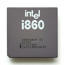
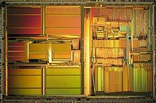
The Intel i860 (also known as 80860) is a RISC microprocessor design introduced by Intel in 1989. It is one of Intel's first attempts at an entirely new, high-end instruction set architecture since the failed Intel iAPX 432 from the beginning of the 1980s. It was the world's first million-transistor chip.[1] It was released with considerable fanfare, slightly obscuring the earlier Intel i960, which was successful in some niches of embedded systems. The i860 never achieved commercial success and the project was terminated in the mid-1990s.
Implementations
[edit] Intel i860 XR microprocessor (33 MHz edition) | |
| General information | |
|---|---|
| Launched | 1989 |
| Discontinued | mid-1990s |
| Common manufacturer |
|
| Performance | |
| Max. CPU clock rate | 25 MHz to 40 MHz |
| Cache | |
| L1 cache | 4 KB (I) + 8 KB (D) |
| Architecture and classification | |
| Instruction set | Intel i860 |
| Physical specifications | |
| Cores |
|
| History | |
| Successor | i860 XP |

 Intel i860 microprocessor (50 MHz edition) | |
| General information | |
|---|---|
| Launched | 1991 |
| Discontinued | mid-1990s |
| Common manufacturer |
|
| Performance | |
| Max. CPU clock rate | 40 MHz to 50 MHz |
| Cache | |
| L1 cache | 16+16 KB |
| Architecture and classification | |
| Instruction set | Intel i860 |
| Physical specifications | |
| Transistors |
|
| Cores |
|
| History | |
| Predecessor | i860 XR |

The first implementation of the i860 architecture is the i860 XR microprocessor (code-named N10), which ran at 25, 33, or 40 MHz. The second-generation i860 XP microprocessor (code named N11) added 4 Mbyte pages, larger on-chip caches, second level cache support, faster buses, and hardware support for bus snooping, for cache consistency in multiprocessor systems. A process shrink for the XP (from 1 μm to 0.8 CHMOS V) increased the clock to 40 and 50 MHz.[3] Both microprocessors supported the same instruction set for application programs.
Technical features
[edit]The i860 combined a number of features that were unique at the time, most notably its very long instruction word (VLIW) architecture and powerful support for high-speed floating-point operations.[4] The design uses two classes of instructions: "core" instructions which use a 32-bit ALU, and "floating-point or graphics" instructions which operate on a floating-point adder, a floating-point multiplier, or a 64-bit integer graphics unit. The system had separate pipelines for the ALU, floating-point adder, floating-point multiplier, and graphics unit. It can fetch and decode one "core" instruction and one "floating-point or graphics" instruction per clock. When using dual-operation floating-point instructions (which transfer values between subsequent dual-operation instructions), it is able to execute up to three operations (one ALU, one floating-point multiply, and one floating-point add-or-subtract) per clock.[1][5]
All of the data buses were at least 64 bits wide. The internal memory bus to the cache, for instance, was 128 bits wide.
The "core" class instructions use thirty-two 32-bit integer registers. But the "floating-point or graphics" instructions use a register file that can be accessed by the floating point units as either thirty-two 32-bit, sixteen 64-bit, or eight 128-bit floating-point registers, or that can be accessed by the graphics unit as sixteen 64-bit integer registers.
The "core" unit is responsible for fetching instructions, and in the normal "single-instruction" mode can fetch one 32-bit "core" or one 32-bit "floating point or graphics" instruction per cycle. But when executing in dual-instruction mode, the instruction cache is accessed as VLIW instructions consisting of a 32-bit "core" instruction paired with a 32-bit "floating-point or graphics" instruction, simultaneously fetched together over a 64-bit bus.[5]
Intel referred to the design as the "i860 64-Bit Microprocessor".[6]
Intel i860 instructions acted on data sizes from 8-bit through 128-bit.[7]
The graphics supports SIMD-like instructions in addition to basic 64-bit integer math. For instance, its 64-bit integer datapath can represent multiple pixels together as either 8-bit pixels, 16-bit pixels, or 32-bit pixels.[5] Experience with the i860 influenced the MMX functionality later added to Intel's Pentium processors.
The pipelines into the functional units are program-accessible (VLIW), requiring the compilers to order instructions carefully in the object code to keep the pipelines filled. In traditional architectures these duties were handled at runtime by a scheduler on the CPU itself, but the complexity of these systems limited their application in early RISC designs. The i860 was an attempt to avoid this entirely by moving this duty off-chip into the compiler. This allowed the i860 to devote more room to functional units, improving performance. As a result of its architecture, the i860 could run certain graphics and floating-point algorithms with exceptionally high speed, but its performance in general-purpose applications suffered and it was difficult to program efficiently (see below).
The i860 has both non-delayed and delayed branch instructions. When delayed branches are taken, the following instruction will be executed prior to transferring control to the branch target instruction. It means the i860 has a single branch delay slot.[8]
Performance
[edit]On paper, performance was impressive for a single-chip solution; however, real-world performance was anything but. One problem, perhaps unrecognized at the time, was that runtime code paths are difficult to predict, meaning that it becomes exceedingly difficult to order instructions properly at compile time. For instance, an instruction to add two numbers will take considerably longer if those numbers are not in the cache, yet there is no way for the programmer to know if they are or not. If an incorrect guess is made, the entire pipeline will stall, waiting for the data. The entire i860 design was based on the compiler efficiently handling this task, which proved almost impossible in practice. While theoretically capable of peaking at about 60-80 MFLOPS for both single precision and double precision for the XP versions,[9] manually written assembler code managed to get only about up to 40 MFLOPS, and most compilers had difficulty getting even 10 MFLOPs.[10] The later Itanium architecture, also a VLIW design, suffered again from the problem of compilers incapable of delivering sufficiently optimized code.
Another serious problem was the lack of any solution to handle context switching quickly. The i860 had several pipelines (for the ALU and FPU parts) and an interrupt could spill them and require them all to be re-loaded. This took 62 cycles in the best case, and almost 2000 cycles in the worst. The latter is 1/20000th of a second at 40 MHz (50 microseconds), an eternity for a CPU. This largely eliminated the i860 as a general purpose CPU.
Demise
[edit]As the compilers improved, the general performance of the i860 did likewise, but by then most other RISC designs had already passed the i860 in performance.
In the late 1990s, Intel replaced their entire RISC line with ARM-based designs, known as the XScale. Confusingly, the 860 number has since been re-used for a motherboard control chipset for Intel Xeon (high-end Pentium) systems and a model of the Core i7.
Andy Grove suggested that the i860's failure in the marketplace was due to Intel being stretched too thin:
We now had two very powerful chips that we were introducing at just about the same time: the 486, largely based on CISC technology and compatible with all the PC software, and the i860, based on RISC technology, which was very fast but compatible with nothing. We didn't know what to do. So we introduced both, figuring we'd let the marketplace decide. ... our equivocation caused our customers to wonder what Intel really stood for, the 486 or i860?
— Andy Grove, [11]
Applications
[edit]
At first, the i860 was only used in a small number of supercomputers such as the Intel iPSC/860. Intel later marketed the i860 as a workstation microprocessor for a time, where it competed with microprocessors based on the MIPS and SPARC architectures, among others. The Oki Electric OKI Station 7300/30[12] and Stardent Vistra 800[13] Unix workstations were based on a 40 MHz i860 XR running UNIX System V/i860.[14] The Hauppauge 4860[15] and Olivetti CP486[16] featured an Intel 80486 and i860 on the same motherboard. Microsoft initially developed what was to become Windows NT on internally designed i860XR-based workstations (codenamed Dazzle), only porting NT to the MIPS (Microsoft Jazz), Intel 80386 and other processors later. Some claim the NT designation was a reference to the "N-Ten" codename of the i860XR.[17]
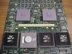
The i860 did see some use in the workstation world as a graphics accelerator. It was used, for instance, in the NeXTdimension, where it ran a cut-down version of the Mach kernel running a complete PostScript stack. However, the PostScript part of the project was never finished so it ended up just moving color pixels around. In this role, the i860 design worked considerably better, as the core program could be loaded into the cache and made entirely "predictable", allowing the compilers to get the ordering right. Truevision produced an i860-based accelerator board intended for use with their Targa and Vista framebuffer cards. Pixar produced a custom version of RenderMan to run on the card that ran approximately four times faster than the 386 host. Another example was SGI's RealityEngine, which used a number of i860XP processors in its geometry engine. This sort of use slowly disappeared as well, as more general-purpose CPUs started to match the i860's performance, and as Intel turned its focus to Pentium processors for general-purpose computing.
Mercury Computer Systems used the i860 in their multicomputer. From 2 to 360 compute nodes would reside in a circuit switched fat tree network, with each node having local memory that could be mapped by any other node. Each node in this heterogeneous system could be an i860, a PowerPC, or a group of three SHARC DSPs. Good performance was obtained from the i860 by supplying customers with a library of signal processing functions written in assembly language. The hardware packed up to 360 compute nodes in 9U of rack space, making it suitable for mobile applications such as airborne radar processing.
During the early 1990s, Stratus Technologies built i860-based servers, the XA/R series, running their proprietary VOS operating system.[18]
Also in the 1990s, Alliant Computer Systems built their i860-based FX/800 and FX/2800 servers, replacing the FX/80 and FX/8 series that had been based on the Motorola 68000 ISA. Both the Alliant and Mercury compute systems were in heavy use at NASA/JPL for the SIR-C missions.
The U.S. military used the i860 for numerous aerospace and digital signal processing applications as a coprocessor, where it saw use up until the late 1990s.[19]
References
[edit]- ^ a b Perry, Tekla (2022-07-02). "The First Million-Transistor Chip: the Engineers' Story". IEEE Spectrum. Archived from the original on 2022-07-05. Retrieved 2022-07-05.
- ^ Lewnes, Ann, "The Intel386 Architecture Here to Stay", Intel Corporation, Microcomputer Solutions, July/August 1989, page 2
- ^ "The i860 XP - Second Generation of the i860" (PDF). Archived from the original (PDF) on 2018-08-20. Retrieved 2015-02-22.
- ^ Kohn, Les; Margulis, N. (August 1989). "Introducing the Intel i860 64-Bit Microprocessor". IEEE Micro. 9 (4). IEEE Computer Society: 15–30. doi:10.1109/40.31485. S2CID 21922034.
- ^ a b c i860 64-bit Microprocessor Programmer's Reference Manual (PDF). Santa Clara, CA, USA: Intel. 1989. Archived (PDF) from the original on 2022-02-23.
- ^ Grimes, Jack; Kohn, L.; Bharadhwaj, R. (July 1989). "The Intel i860 64-Bit Processor: A General-Purpose CPU with 3D Graphics Capabilities". IEEE Computer Graphics and Applications. 9 (4). IEEE Computer Society: 85–94. doi:10.1109/38.31467. S2CID 38831149.
- ^ "The Chip Collection - i860 Microprocessor - Smithsonian Institution". Smithsonian Institution.
- ^ "i860™ 64-bit Microprocessor Programmer's Reference Manual" (PDF). p. 70(5-11). Retrieved 2023-12-21.
- ^ Oleg Yu. Repin, Alexei S. Pylkin (2000). "Intel i860 : 64-Bit Microprocessor". sscc.ru, ICMMG. Archived from the original on 2009-06-23. Retrieved 2013-09-27.
- ^ Bailey, D.H.; Barszcz, E.; Fatoohi, R.A.; Simon, H.D.; Weeratunga, S. (1990). Performance Results on the Intel Touchstone Gamma Prototype (PDF) (Report). NASA Ames Research Center. Archived from the original (PDF) on 2016-12-21. Retrieved 2016-07-10.
- ^ Olson, Sander (3 June 2004). "Intel's 486 CPU turns 15". Geek.com. Archived from the original on 2008-05-25.
- ^ "Oki Electric OKI Station 7300/30-Computer Museum".
- ^ "Intel i860 - From Here to There". 2010.
- ^ "KUBOTA Computer/Stardent AVSstation Titan Vistra 800". Archived from the original on 2014-05-14. Retrieved 2014-05-14.
- ^ "GeekDot - Hauppauge 4860". 20 March 2008.
- ^ "GeekDot - Olivetti CP486". 16 August 2011.
- ^ Thurrott, Paul (2003-01-24). "Windows Server 2003: The Road To Gold". Win super site. Archived from the original on 2011-07-20. Retrieved 2013-09-02.
- ^ "Stratus Machine History". Archived from the original on 2003-06-12.
- ^ "StackPath". May 1997.
- Margulis, Neal (1990). i860 Microprocessor Architecture. Osborne/McGraw-Hill. ISBN 978-0-07-881645-1.
External links
[edit]- Many i860 expansion cards
- i860 images and description.
- Rhodehamel, Michael W. (1989). "The bus interface and paging units of the i860 microprocessor". Proceedings 1989 IEEE International Conference on Computer Design: VLSI in Computers and Processors. Cambridge, MA, USA. pp. 380–384. doi:10.1109/ICCD.1989.63392.
