Field-emission microscopy
Field-emission microscopy (FEM) is an analytical technique that is used in materials science to study the surfaces of needle apexes.[1][2] The FEM was invented by Erwin Wilhelm Müller in 1936,[3] and it was one of the first surface-analysis instruments that could approach near-atomic resolution.
Introduction
[edit]Microscopy techniques are utilized to generate magnified real-space images of the surface of a tip apex. Typically, microscopy information pertains to the surface crystallography (i.e., how the atoms are arranged at the surface) and surface morphology (i.e., the shape and size of topographic features making the surface).
Field-emission microscopy (FEM) was invented by Erwin Müller in 1936.[3] In FEM, the phenomenon of field electron emission was used to obtain an image on the detector based on the difference in work function of the various crystallographic planes on the surface.
Setup and working principle
[edit]
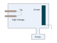
A field-emission microscope consists of a metallic sample shaped like a sharp tip and a fluorescent screen enclosed within an ultrahigh vacuum chamber. Typically, the tip radius used in this microscope is on the order of 100 nm, and it is made of a metal with a high melting point, such as tungsten.[4] The sample is held at a large negative potential (1–10 kV) relative to the fluorescent screen, which generates an electric field near the tip apex of 2-7 x 10⁹ V/m. This electric field drives field emission of electrons.
The field-emitted electrons travel along the field lines and produce bright and dark patches on the fluorescent screen, exhibiting a one-to-one correspondence with the crystal planes of the hemispherical emitter. The emission current strongly varies with the local work function, following the Fowler–Nordheim equation. Therefore, the FEM image reflects the projected work function map of the emitter surface. Generally, atomically rough surfaces have lower work functions than closely packed surfaces, resulting in bright areas in the image. In short, the intensity variations of the screen correspond to the work function map of the surface of the tip apex.
The magnification is given by the ratio , where is the tip apex radius, and is the tip–screen distance. Linear magnifications of the order of 105 are attained. The FEM technique has a spatial resolution of around 1 - 2 nm.[2] Nonetheless, if a particle with a size of 1 nm is placed on a tip apex, the magnification can increase by a factor of 20, and the spatial resolution is enhanced to approximately 0.3 nm.[5] This situation can be achieved by utilizing single-molecule electron emitters,[6] and it is possible to observe molecular orbitals in single fullerene molecules using FEM.[7]
Application of FEM is limited by the materials that can be fabricated in the shape of a sharp tip and can tolerate high electrostatic fields. For these reasons, refractory metals with high melting temperatures (e.g., W, Mo, Pt, Ir) are conventional objects for FEM experiments. In addition, the FEM has also been used to study adsorption and surface diffusion processes, making use of the work-function change associated with the adsorption process.
See also
[edit]References
[edit]- ^ "Intro to Field Emission". Field Emission / Ion Microscopy Laboratory, Purdue University, Dept. of Physics. Archived from the original on 2007-05-03. Retrieved 2007-05-10.
- ^ a b Field Emissions and Field Ionization.
- ^ a b Müller, Erwin W. (November 1936). "Die Abhängigkeit der Feldelektronenemission von der Austrittsarbeit". Zeitschrift für Physik (in German). 102 (11–12): 734–761. doi:10.1007/BF01338540. ISSN 1434-6001.
- ^ Stranks, D. R.; M. L. Heffernan; K. C. Lee Dow; P. T. McTigue; G. R. A. Withers (1970). Chemistry: A structural view. Carlton, Victoria: Melbourne University Press. p. 5. ISBN 0-522-83988-6.
- ^ Rose, D. J. (March 1956). "On the Magnification and Resolution of the Field Emission Electron Microscope". Journal of Applied Physics. 27 (3): 215–220. doi:10.1063/1.1722347. ISSN 0021-8979.
- ^ Yanagisawa, Hirofumi; Bohn, Markus; Goschin, Florian; Seitsonen, Ari P.; Kling, Matthias F. (2022-02-17). "Field emission microscope for a single fullerene molecule". Scientific Reports. 12 (1): 2714. doi:10.1038/s41598-022-06670-1. ISSN 2045-2322. PMC 8854663. PMID 35177727.
- ^ Yanagisawa, Hirofumi; Bohn, Markus; Kitoh-Nishioka, Hirotaka; Goschin, Florian; Kling, Matthias F. (2023-03-08). "Light-Induced Subnanometric Modulation of a Single-Molecule Electron Source". Physical Review Letters. 130 (10): 106204. doi:10.1103/PhysRevLett.130.106204.


